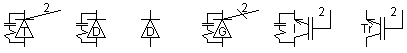
This component models one of the following power electronic devices:
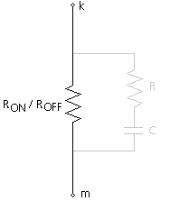
All devices are represented as a two-state resistive switch with an optional RC snubber connected in parallel with the device, as shown below:
The Thyristor, GTO and IGBT models require an input gating pulse and can be applied to high frequency switching and pulse width modulation power electronic circuits. Interpolated firing pulses can be supplied to these devices by using the Interpolated Firing Pulses component. In simulations such as Voltage Source Converters or other FACTS devices, care must be taken in ensuring the observed losses are realistic.
The Interpolation Algorithm is automatically invoked during all naturally commutated turn ON and turn OFF events (including forward break-over) in order to calculate the exact instant of switching. Please note however, that device turn ON or OFF using a gate signal is not interpolated unless specifically selected in the input parameters.
More: |
Name for Identification |
Text |
Optional text parameter for identification of the component. |
||
Device Label (optional) |
|
Text |
|
An optional text label. The contents of this input will be displayed directly on the component graphic |
|
|
|
|
|
Device Type |
|
Choice |
|
Select Diode, Thyristor, GTO, IGBT or Transistor. |
|
|
|
|
|
Enable Snubber Circuit? |
|
Choice |
|
Select Yes or No |
|
|
|
|
|
Interpolated Pulse? |
|
Choice |
|
Select Yes or No |
Thyristor ON Resistance |
|
REAL |
Constant |
Resistance of device when in the ON state (conducting) [W] |
|
|
|
|
|
Thyristor OFF Resistance |
|
REAL |
Constant |
Resistance of device when in the OFF state [W] |
|
|
|
|
|
Forward Voltage Drop |
|
REAL |
Constant |
Forward voltage drop of device. This input may be 0.0 [kV] |
|
|
|
|
|
Forward Breakover Voltage |
|
REAL |
Constant |
Forward break-over voltage of device. Device will be forced into conduction if this voltage is exceeded (with or without a gate pulse) [kV] |
|
|
|
|
|
Reverse Withstand Voltage |
|
REAL |
Constant |
Reverse withstand voltage of device. Device will be forced into conduction in the reverse direction if this voltage is exceeded [kV] |
|
|
|
|
|
Minimum Extinction Time |
|
REAL |
Constant |
Minimum extinction time of device. Device will re-fire if the voltage exceeds Forward Voltage Drop within the this time since last turn off [ms] |
|
|
|
|
|
Snubber Resistance |
|
REAL |
Constant |
Enter a value for snubber resistance. See Snubber Circuit for more details [W] |
|
|
|
|
|
Snubber Capacitance |
|
REAL |
Constant |
Enter a value for snubber capacitance. See Snubber Circuit for more details [mF] |
|
|
|
|
|
Protected Against Forward Break-over? |
|
Choice |
|
Select Yes or No.
If Yes is selected, a 'fake' firing pulse is issued to the switch just before the breakdown occurs, thereby protecting the switch. If it set to No, permanent breakdown may occur. |
Internal Output VariablesInternal Output Variables
Current in Device (Snubber Excluded) |
|
REAL |
Output |
[kA] |
|
|
|
|
|
Total Current in Device |
|
REAL |
Output |
[kA] |
|
|
|
|
|
Voltage Across the Device |
|
REAL |
Output |
[kV] |
|
|
|
|
|
Time of Last Turn On |
|
REAL |
Output |
[s] |
|
|
|
|
|
Time of Last Turn Off |
|
REAL |
Output |
[s] |
|
|
|
|
|
Alpha in Seconds |
|
REAL |
Output |
[s] |
|
|
|
|
|
Gamma in Seconds |
|
REAL |
Output |
[s] |