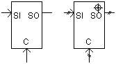
This N-bit, serial in/serial out shift register is constructed with N, D Flip-Flops connected in cascade, with the output Q of one flip-flop connected to the input D of the next flip-flop to its right as shown below for a 4-bit register:

In order to shift the register from one stage to the next, a common clock pulse C is received by all flip-flops. The clock-pulse input causes the serial input SI to go into the left-most flip-flop and the serial output SO is taken from the output of the right-most flip-flop. All the contents of the register are shifted one bit to the right.
The state of the register changes depending on the value of C. If C is chosen as falling, the output changes state only on the falling edge of a clock pulse. If it is chosen as rising, the output changes state only on the rising edge of a clock pulse.
If Interpolation Compatibility is enabled, then the relevant interpolated information, from either the input or the clock, is passed between the internal devices. In addition, the interpolated information is used to determine the internal flip-flop logic according to the exact instants in which the inputs, outputs and the clock signals transition. When full interpolation is utilized, this device is very accurate even at larger time steps.
More: |
Name for Identification |
Text |
Optional text parameter for identification of the component. |
||
Number of Bits |
|
Choice |
|
Select the number bits for this register from 2 to 8 |
|
|
|
|
|
Active Clock Edge |
|
Choice |
|
Select Negative [1->0] or Positive [0->1]. This input indicates what part of the clock signal will be used to activate a flip-flop transition. These are falling and rising edge respectively. |
|
|
|
|
|
Interpolation Compatibility |
|
Choice |
|
Select Disable or Enable. See Description for more details. |
InitializationsInitializations
Initial State of Output |
|
Choice |
|
Select the initial state of each internal output |